
ASML Hyper NA Research Targets 5-Nanometer Chip Features
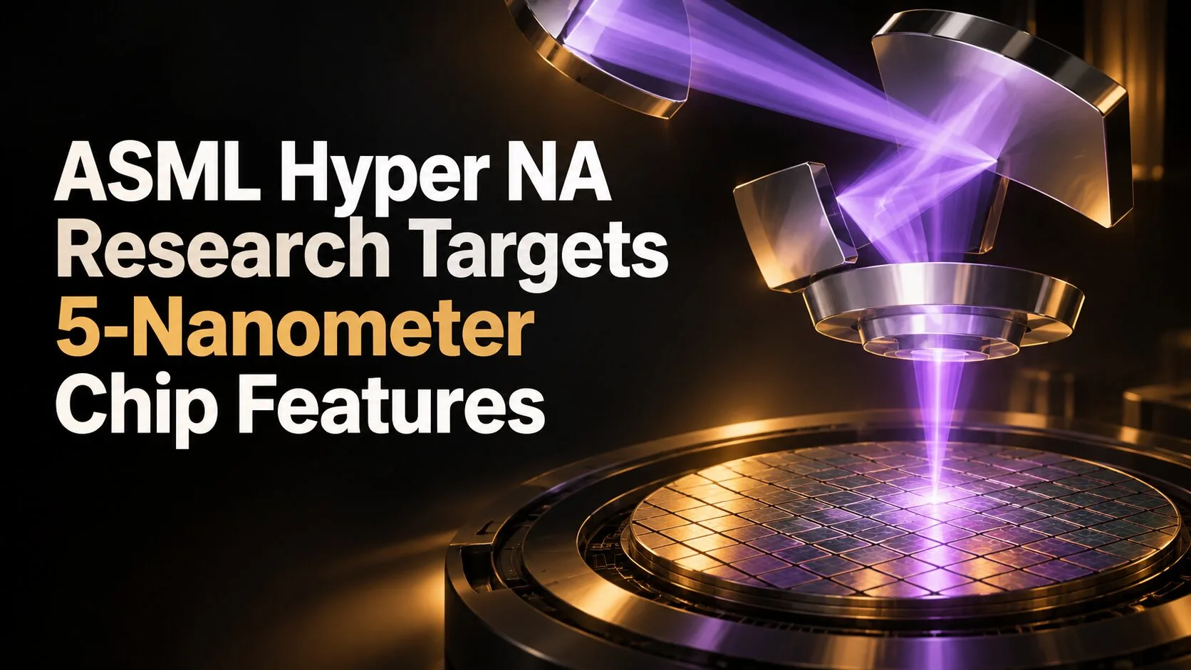
ASML Hyper NA research has outlined a successor to today’s most advanced chipmaking equipment, targeting features as small as 5 nanometers. Engineers from ASML and Carl Zeiss describe an extreme-ultraviolet lithography system with a numerical aperture of at least 0.75 that could be ready in roughly a decade.
The proposed system rests on four concrete advances:
- At least 0.75 numerical aperture
- About 5-nanometer half-pitch resolution
- Reuse of the current EUV light source
- Mirrors within Zeiss’s manufacturing capability
ASML Hyper NA Raises Numerical Aperture to 0.75
ASML’s existing High NA platform uses a 0.55 numerical aperture, already a major step beyond conventional EUV equipment. Numerical aperture describes how much light an optical system can collect and focus. Raising it lets a lithography machine resolve finer patterns on a silicon wafer.
The October paper, published in the Journal of Micro/Nanopatterning, Materials, and Metrology, examines a Hyper NA architecture with a numerical aperture of at least 0.75. Its authors work at Carl Zeiss SMT and ASML, the two companies responsible for the projection optics and complete EUV lithography systems.
The proposed 5-nanometer half-pitch would be more than one-third smaller than the features possible with High NA. That does not translate directly into a commercial “5nm process node,” because marketing node names no longer correspond to one physical dimension. It instead describes the pitch the exposure system is designed to resolve.
Smaller printed features remain valuable even as chipmakers increasingly stack components in three dimensions. Denser transistors and interconnects can improve performance and energy efficiency, both central constraints for AI accelerators that consume large amounts of power while moving data between compute engines and memory.
Zeiss Mirrors and Existing EUV Sources Reduce the Redesign
The paper’s most practical claim is not simply that higher resolution is physically possible. The authors argue that much of today’s EUV ecosystem can carry forward, lowering the number of technologies that must be replaced simultaneously before Hyper NA can become a manufacturing platform.
Zeiss can already manufacture mirrors precise enough for the optical design, according to the researchers. EUV lithography depends on reflective optics because its 13.5-nanometer light is absorbed by conventional lenses. Any increase in aperture therefore requires exceptionally accurate mirrors, coatings and alignment across the projection system.
ASML’s current EUV light source can also be reused without modification, the paper says. That is significant because generating stable, high-power EUV light was one of the hardest engineering problems behind the original technology. Reusing the source narrows Hyper NA’s challenge to optics, masks, resist materials, polarization and system integration.
The proposed tool would be only slightly larger than a High NA system, which already approaches the size of a double-decker bus. A familiar footprint matters because leading-edge fabs are planned around strict limits for floor space, vibration control, power, water, service access and wafer movement.
High NA Adoption Sets the Commercial Timeline
Hyper NA is not a committed product. ASML has begun development, Reuters reported, but the company has not promised to manufacture or sell the machine. The decade-long estimate reflects both the technical work and the industry coordination required before chipmakers can use a new lithography generation at acceptable cost and yield.
High NA itself is only beginning commercial adoption. Intel has started using the platform in production and said in September that it had processed more than one million wafers. Samsung and SK Hynix plan to introduce High NA in 2028, while TSMC has set a 2030 target.
Those schedules place Hyper NA after customers have spent years learning how to operate its predecessor. Tool builders, mask suppliers, chemical companies and chip manufacturers must jointly refine exposure recipes, photoresists, defect inspection and process control before a laboratory capability can support high-volume production.
Economics will matter as much as resolution. Current High NA systems cost about $400 million, roughly twice the price of conventional EUV machines. Hyper NA must therefore deliver enough performance, power or process-step savings to justify another expensive equipment transition rather than relying solely on better packaging and three-dimensional designs.
Hyper NA Extends EUV Before a New Wavelength
The research gives the semiconductor industry a possible route to extend EUV without immediately changing its 13.5-nanometer wavelength. That preserves years of investment in sources, masks, materials and factory infrastructure while asking optics to carry another major increase in resolution.
Beyond Hyper NA, the authors expect that further progress would probably require shorter-wavelength light. That remains an academic research problem and would force a broader reset of the exposure ecosystem. Competing approaches, including free-electron lasers and X-ray lithography, are being studied but are not yet established production alternatives.
For AI hardware, the paper is a long-range signal rather than an immediate capacity increase. It suggests ASML and Zeiss see a credible optical path beyond High NA, but commercial evidence will depend on manufacturability, throughput, defect rates and customer economics over the next decade.
If the architecture reaches production, Hyper NA could preserve conventional transistor scaling alongside chiplets and advanced packaging. The important milestone is not the paper’s 5-nanometer figure alone; it is the claim that the next resolution step can reuse critical parts of the EUV platform already moving into leading fabs.
Related Coverage